

Company News

Fudan University cooperates with Lattice Power Semiconductor to report for the first time the research results of silicon substrate InGaN red light Micro-LED for visible light communication
Recently, Fudan University and Jiangxi Lattice Power Semiconductor collaborated on the research results on the application of silicon-based InGaN red light Micro-LED in multi-color displays and high-speed visible light communications. The title "Red InGaN Micro-LEDs on Silicon Substrates: Potential for Multicolor Display and Wavelength Division Multiplexing Visible Light Communication" was published in the top international journal in the field of optical communications "Lightwave Technology Magazine" (IEEE/OSA Journal of Lightwave Technology). After the results were published, the famous international semiconductor industry magazine "Semiconductor Today" published a column titled "Red InGaN LEDs for visible light communication" (Red InGaN LEDs for visible light communication) report, stating that "Fudan University and Jiangxi Lattice Power Semiconductor reported for the first time red-emitting micro-light-emitting diodes on silicon substrates for visible light communications. The team also studied the wavelength/color of micro-LEDs of various sizes as a function of current of red to green for display and multi-wavelength data transmission."
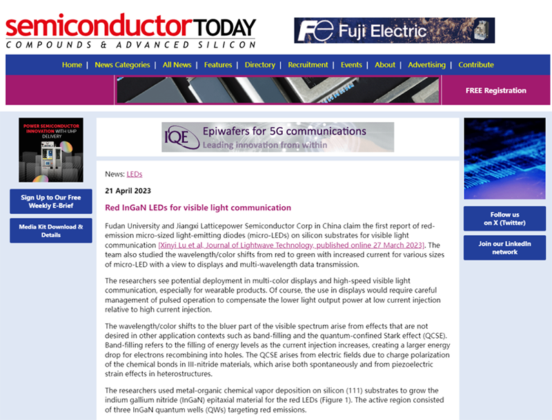
Figure 1 Screenshot of "Semiconductor Today" report.
Micro-LED, as an emerging technology, shows great potential in next-generation advanced display systems, visible light communications and optogenetics. Compared with mature green and blue GaN material systems, the development of red Micro-LEDs faces huge challenges. Commonly the red LEDs are made of aluminum indium gallium phosphide (AlInGaP) material, but as the chip size shrinks to the micron level, the efficiency of AlInGaP-based Micro-LEDs will significantly decrease. In addition, AlInGaP is incompatible with existing GaN-based green and blue LED material systems. Theoretically, InGaN materials can cover the entire visible spectrum by adjusting the indium content in multiple quantum wells, and have good mechanical stability and higher potential efficiency, and gradually becoming an ideal material for micron-level red light emission.
Currently, InGaN red Micro-LEDs are mostly grown on patterned sapphire substrates or introduce GaN pseudo-substrates on sapphire substrates. If applied to transfer-printed display technology, a relatively expensive laser lift-off process is required to remove the native substrate. As a growth substrate with great commercial application potential, silicon can obtain large-area, high-quality wafers at low manufacturing costs. However, so far, there are few reports on silicon substrate InGaN red Micro-LED, lacking detailed research on its device performance and application fields.
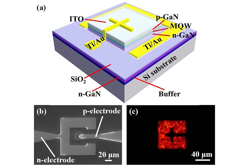
To this end, the research team selected silicon substrate InGaN red Micro-LED as the research object and analyzed the wavelength/color changes of pixels of different sizes as the current increases to achieve multi-color display and multi-wavelength data transmission (Figure 2). By adjusting the pixel size and injecting current, a significant blue shift phenomenon was observed, with the wavelength shifting from red light to green light. At a high current density of 100 A/cm2, the peak wavelength of all pixels exceeds 630 nm, which can meet application scenarios that require high current density, such as augmented reality, virtual reality and other fields. As the current density increases, the CIE coordinates also shift from the red light area to the green light area, showing a wider color gamut. Multi-color light emission with uniform brightness is achieved by adjusting the duty cycle, demonstrating its application potential in single-chip, multi-color micro-LED displays. Subsequently, the display characteristics of the 80 μm pixel were discussed in detail. At a low current density of 2 A/cm2, the EQE reached 0.19%, and at a current density of 100A/cm2, the EQE was 0.14%.
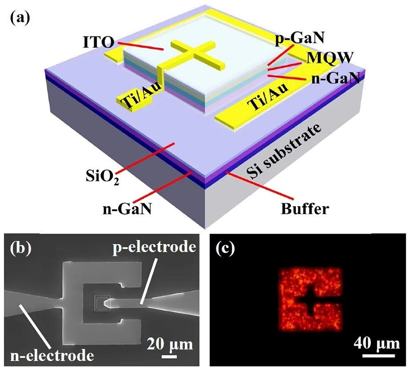
Figure 2 (a) Schematic diagram of the structure of a top-emitting Micro-LED device; (b) SEM photo of the prepared 20μm red light pixel; (c) Optical microscope photo of an 80 μm red pixel at a current density of 20 A/cm2.
The researchers further tested the communication performance of red pixels of different sizes and found that the modulation bandwidth of InGaN red Micro-LEDs (size less than 100 μm) on silicon substrates exceeded 400 MHz, making them very suitable for data transmission (Figure 3). For a 40μm pixel, the maximum modulation bandwidth that can be achieved when emitting red light, yellow light, and green light is 112.67 MHz, 126.38 MHz, and 533.15 MHz respectively. Among them, the modulation bandwidth achieved when green light is emitted is the record bandwidth of color-tunable Micro-LEDs reported so far, demonstrating its huge advantages in multi-color visible light communications.
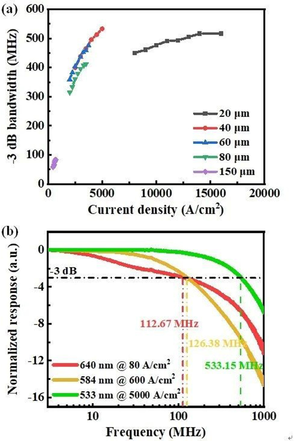
Figure 3 (a) -3dB modulation bandwidth as a function of current density for all pixel sizes. (b) Frequency response curves of 40μm pixels at 80, 600 and 5000 A/cm2, corresponding to the wavelengths of 640 nm (red light), 584 nm (yellow light) and 533 nm (green light) respectively.
Subsequently, a single-chip, multi-color wavelength division multiplexing scheme was proposed (Figure 4). Micro-LEDs with different emission wavelengths are used at the transmit end of visible light communication, with the maximum allowed transmission data rate reaching 2.35 Gbps. This is the first report of silicon substrate InGaN red light Micro-LED being used in visible light communication. Due to the high integration and miniaturization of pixels, this device has great application potential in fields such as wearable communication devices and smart watches, and is expected to reduce the complexity of overall system integration in the future.
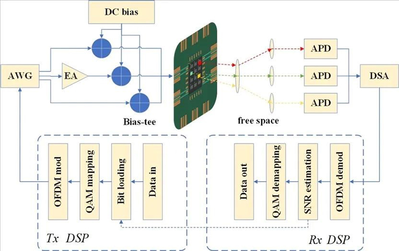
Figure 4 Schematic diagram of the experimental device of the WDM-OWC system.
Related Links:
Paper link: https://doi.org/10.1109/JLT.2023.3261875
Column report link: https://www.semiconductor-today.com/news_items/2023/apr/fudan-210423.shtml